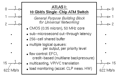
Figure 1: ATLAS I chip overview
Institute of Computer Science (ICS)
Foundation for Research and Technology -- Hellas (FORTH)
Science and Technology Park of Crete,
P.O.Box 1385, Heraklion, Crete, GR 711 10 Greece
most authors are or were also with the
Department of Computer Science,
University of Crete, Greece.
Proceedings of the
IEEE Hot Interconnects VI Symposium,
Stanford University, California USA, 13-15 August 1998
© Copyright 1998 IEEE
[ Up to the ATLAS I Home Page ]
ABSTRACT:
ATLAS I is a single-chip ATM switch with
10 Gb/s throughput, a shared buffer, 3 priority levels,
multicasting, load monitoring, and optional credit-based flow control.
This 6-million-transistor 0.35-micron CMOS chip
is about to be taped out for fabrication.
We present here the implementation of ATLAS I;
we report on the design complexity and silicon cost
of the chip and of the individual functions that it supports.
Based on these metrics,
we evaluate the architecture of the switch.
The evaluation points in the direction of
increasing the cell buffer size and
dropping VP/VC translation,
while other possible modifications are also discussed.
The cost of credit support (10% in chip area and 4% in chip power)
is minuscule compared to its benefits,
i.e. compared to what alternative architectures have to pay
in order to achieve comparable performance levels.
KEYWORDS: single-chip ATM switch, general-purpose building block for universal networking, credit-based flow control, backpressure, VLSI switch implementation cost & evaluation.
This paper presents the design complexity and implementation cost of the chip and of the various functions in it, and evaluates the switch in view of these metrics. We estimate the design complexity in terms of (Verilog) code size and (approximate) human effort. We measure the implementation cost in terms of gates, flip-flops, and SRAM bit counts, silicon area, and power consumption. We break these metrics down by function supported, rather than by hardware block. Then, we proceed to evaluate the design style and library used: semi-custom versus full-custom, and compiled memory availability. Finally, we evaluate the architecture of the switch, in view of the design metrics. We look at the functions that turned out to have a high cost, and discuss how a different organization could lower this cost, or whether they should rather be dropped. In particular, we discuss backpressure, and show why its important benefits are well worth its cost.
Figure 1: ATLAS I chip overview
The most distinctive and innovative feature of ATLAS I is its (optional) provision of credit-based flow control (backpressure), using a protocol that resembles QFC [QFC95] but is adapted to hardware implementation. A cell in a backpressured service class (priority level) can only depart if it acquires both a buffer-pool credit for its outgoing link and a flow-group credit for its connection. A flow group is a set of connections that are flow-controlled together; ATLAS I supports up to 32 thousand flow groups (2048 per link). Credits are transmitted on the links using 1 control and 3 data characters for each of them. Credit-based flow control is useful in building switching fabrics with internal backpressure that provide the high performance of output queueing at the low cost of input buffering [KaSS97], and in making ATM sub-networks that never drop cells of data connections while fully and fairly utilizing all the available transmission capacity, so as to provide the lowest possible message delivery time. Our evaluation of the credit protocol has shown its superior performance, especially in isolating well-behaved connections from bursty and hot-spot traffic [KaSS98].
In the rest of this paper, when breaking down the chip cost by function, we use the following list of functions provided by ATLAS I. These can also be seen in the floorplan of the chip, in figure 2.

Figure 2: Floorplan of the ATLAS I chip
The synthesis was performed hierarchically, using the natural block boundaries that are defined both by functionality and by the pipeline partitioning. These boundaries dictate the general floorplan of the ATLAS I switch core. The hierarchical compilation permits a hierarchical placement of the cells in the larger blocks, allowing short interconnect delays. At the top level of the hierarchy, 15 blocks were defined, and placement and routing was performed individually, for each of them. Within each of these 15 blocks, the hierarchy is removed after placement and before routing; this is to allow for global clock-tree generation, and in order to minimize the rather lengthy setup time of the routing tools.
The back-end design flow was as follows. First, the top floorplan and the block floorplans were made, using the Cadence environment, after importing the EDIF netlist. Next, for each block, placement and routing is performed with Cell3, using the EDIF netlist and the block floorplan. Back-annotation follows, in order to calculate the clock skew and the overloads; these are fed back to Synopsys for in-place optimization and fix. A new round starts with Cell3 (ECO), to incrementally fix the placement and routing, and so on until no more changes are needed. Final verification (DRC, LVS) is performed using Dracula.
One ATLAS I block was laid-out in full-custom; it performs key functions for queue management and credit-based flow control, and was described in [Korn97]. The functions required are multiport (3 and 4 port) SRAMs, content addressable memories (CAMs), and memories with simultaneous read and modify accesses, which can not be generated automatically by a silicon compiler. Together with their peripheral circuitry, they were laid-out using the Cadence Virtuoso editor, and were verified for function and timing at the transistor level with ELDO simulations. At the logic level, we used IRSIM to verify this block.
The design cost of the main ATLAS I functions is shown in table 1. Code size, in thousands of Verilog lines, refers to the structural model that was used for synthesis. The code is very dense and compact, since it uses all the basic hardware components from a large internally developed library. The figures in table 1 do not include: the component library (2 Klines), the behavioral models of the full-custom blocks (3.2 Klines), and our test environment (3.4 Klines of Verilog and 5 Klines of PERL).
| Function: | Verilog | Synth. | Human Effort | |
|---|---|---|---|---|
| K lines | hours | p-yrs | % | |
| Buffer | 1.0 | 5 | 1.0 | 7 |
| Queue Mgt. | 1.4 | 2 | 2.3 | 15 |
| Rt'ng/Tran. | 2.1 | 12 | 2.2 | 15 |
| Sched. Cnt. | 1.5 | 18 | 2.0 | 13 |
| Ctrl. Mgt. | .7 | 6 | 1.0 | 7 |
| Credits | 1.0 | 7 | 3.0 | 20 |
| Load Mon. | .4 | 24 | .5 | 3 |
| Elastic I/F | 3.6 | 22 | 2.0 | 13 |
| Miscellany | 1.8 | 4 | 1.0 | 7 |
| Total | 13.5 | 100 | 15. | 100% |
The second column of the table lists the time required to synthesize the Verilog code of the blocks into gate level descriptions, on a SUN Ultra-2 with a 200 MHz processor and 384 Mbytes of main memory. This main memory size was sufficient for the synthesis of each individual block, so the reported time was spent entirely on synthesis optimizations. The synthesis times are relatively small, but they are the result of an extensive trial and error process in which more than 1,000 hours of CPU time were spent to establish the best paramenters and balance the constraints among different blocks of logic. We found that the hierarchical compilation process does speed synthesis up considerably, and gives better results than a flat one, but only after a long experimentation phase and considerable manual labor for tuning. We also found that the automatic hierarchical compilation scripts were only successful for the parts of the switch that were both small and relatively simple.
The last two columns of table 1 show the approximate human effort spent for the entire ATLAS I core design. This includes both full-custom and semi-custom design, synthesis, simulation, timing verification, placement, routing, back-annotation. The total effort was 15 person-years, or an average of 6 full-time-equivalent persons working for 2.5 years (early 1996 through mid 1998). The figures in table 1 do not include the architectural design of the switch, which went on in 1995.
| Function: | Gates | Flip-Flops | SRAM | |||
|---|---|---|---|---|---|---|
| K | % | K | % | Kbits | % | |
| Buffer | 28 | 19 | 9.6 | 22 | 120 | 21 |
| Queue Mgt. | 12 | 8 | .9 | 2 | 10 | 2 |
| Rt'ng/Tran. | 20 | 13 | 9.2 | 21 | 300 | 53 |
| Sched. Cnt. | 4 | 3 | .7 | 2 | 1 | 0 |
| Ctrl. Mgt. | 2 | 1 | .3 | 1 | 1 | 0 |
| Credits | 15 | 10 | 2.3 | 5 | 134 | 24 |
| Load Mon. | 4 | 3 | 1.6 | 3 | 0 | 0 |
| Elastic I/F | 65 | 43 | 19.4 | 44 | 0 | 0 |
| Total | 150 | 100% | 44.0 | 100% | 566 | 100% |
Table 3 breaks down the silicon area cost of ATLAS I by function. The transceivers account for 1/4 of the chip, and the core occupies 2/3 of the chip. One third of the core is taken up by (mostly uncompacted) global routing and power rails; this area includes our ``safety margin'' --the external dimensions of the chip were fixed a priori. The core is taken up by three --almost equal-sized-- functions: buffer, routing/translation, credits. The link interfaces & elastic buffers form a fourth, smaller function, while all other functions occupy very small area.
| Function: | Logic | SRAM | Routing | Total | |
|---|---|---|---|---|---|
| mm² | mm² | mm² | mm² | % | |
| Buffer | 5.1 | 8.4 | 9.5 | 23.0 | 10 |
| Queue Mgt. | 1.4 | 1.0 | .7 | 3.1 | 1 |
| Rt'ng/Tran. | 5.6 | 11.7 | 5.6 | 22.9 | 10 |
| Sched. Cnt. | .5 | .9 | .9 | 2.3 | 1 |
| Ctrl. Mgt. | .2 | .4 | .2 | .8 | 0 |
| Credits | 2.2 | 14.6 | 8.0 | 24.8 | 11 |
| Load Mon. | 1.0 | .0 | .4 | 1.4 | 1 |
| Elastic I/F | 10.7 | .0 | 3.0 | 13.7 | 6 |
| Total Blocks | 26.7 | 37.0 | 28.3 | 92. | 41 |
| Glob. Rout. | 54. | 54. | 24 | ||
| Total Core | 82. | 146. | 65 | ||
| Transceivers | 57. | 25 | |||
| Pads, Driv. | 22. | 10 | |||
| Total Chip | 225. | 100 | |||
Table 4 shows the power dissipation of the ATLAS I blocks. Off-chip communication consumes half of the 9 Watt chip power, with the Gigabaud transceivers consuming the large majority of that. In the core, more than half of the power goes to the buffer memory which also performs the switching. This is reasonable, in view of the fact that, in each clock cycle, 480 bits are read or written to/from the memories in this block. The other functions consume much smaller amount of power, each.
| Function: | Logic | SRAM | Total | |
|---|---|---|---|---|
| mW | mW | W | % | |
| Buffer | 1,040 | 1,360 | 2.40 | 27 |
| Queue Mgt. | 60 | 170 | .23 | 3 |
| Rt'ng/Tran. | 410 | 250 | .66 | 7 |
| Sched. Cnt. | 40 | 120 | .16 | 2 |
| Ctrl. Mgt. | 10 | 2 | .01 | 0 |
| Credits | 190 | 180 | .37 | 4 |
| Load Mon. | 100 | 0 | .10 | 1 |
| Elastic I/F | 280 | 0 | .28 | 3 |
| Total Core | 2,130 | 2,080 | 4.2 | 47 |
| Transceivers | 4.0 | 44 | ||
| Pads, Driv. | .8 | 9 | ||
| Total Chip | 9.0 | 100% | ||
| elastic buffer (incoming) | 10 cycles |
| header proc., routing/transl. | 10 cycles |
| enqueue, schedule-out, dequeue | 5 cycles |
| buffer memory read & switch | 3 cycles |
| elastic buffer (outgoing) | 2 cycles |
| Total Cut-Through Delay | 30 cycles |
|---|---|
This delay is longer than originally intended, and most of it is due to secondary effects rather than intrinsic, core functions; in the next sections we discussed how it could be reduced. Elastic buffer delay is discussed in sections 5.3 and 6.5. Header processing and routing/translation delay is broken down as follows: 3 cycles for header generation (assemble a 5-byte header from a 2-byte/cycle datapath); 2 cycles for the header serializer (to maintain arrival order, which is important for link bundling); 2 cycles for header pattern matching (CAM); and 3 cycles for routing/translation. These header processing delays are discussed in sections 5.2 and 5.4.
In retrospect, it would have been desirable for the ATLAS I cell buffer capacity to be 512 or 1024 ATM cells i.e. two to four times larger than it is now. Such a capacity increase would lead to less than twice or four times the buffer SRAM area --currently 8.4 mm² (SRAM area is a sublinear function of capacity), while the peripheral circuits of the buffer would not be significantly affected. The resulting area increase of roughly 8 or 20 mm² could be absorbed by reducing the header processing area (section 5.2), or by better compaction of the 54 mm² global routing area, or with a full-custom pipelined memory implementation (section 4). The cell buffer consumes considerable power --one fourth of the entire chip-- but this is due mostly to the peripheral circuits and to the number of bits read/written per cycle (30 memories x 16 bits/memory = 480 bits), so it would not increase much when increasing just the number of words per memory.
ATLAS I provides VP/VC translation because the standards specify that an ATM switch must provide that function. On the other hand, our analysis of network addressing mechanisms (see [Man97]) indicates that translation is not necessary in small ATM (sub-) networks, while large ATM networks need large VP/VC translation tables; furthermore, large translation tables cannot be synthesized as a cascade of multiple small tables in successive stages of switching fabrics. Therefore, the --necessarily small-- translation table in ATLAS I is not very useful: large networks need off-chip memory to implement translation, while small networks do not need translation.
VP/VC translation costs in multiple respects: (i) the translation table occupies about 1/4 of the header processing area; (ii) header pattern matching occupies another 1/4 of the block's area --the function of this 40-entry CAM is to provide a high degree of configurability regarding the ATM standard VP/VC switching modes; (iii) the large number of sequential header processing steps resulted in an excessive number of clock cycles being spent for these functions (section 3.3) --the 5 clock cycles of latency that are due to routing and translation would have been reduced to 2 cycles if translation were not performed and less configurability options were provided. We conclude from the above that, for someone who wanted to simplify ATLAS I or needed a larger cell buffer and did not have the silicon area for that, the first priority would be to eliminate VP/VC translation from the chip functions.
To achieve (almost) this rate we would have to use a 13-bit datapath; besides being unconventional, this would complicate the conversion between the byte-oriented HIC/HS link protocol and the internal datapath. Instead, we decided to use 16-bit internal datapaths. This, however, means that the pipelined memory ``absorbs'' an incoming cell in 53/2 ~= 27 clock cycles, or 27/33 = 82% of a cell-time. The pipelined memory --as well as cut-through operation-- need an uninterrupted flow of incoming data, for each cell. It follows that the pipelined memory can only start receiving an incoming cell 33-27 = 6 clock cycles after cell arrival on the link. This initial delay of 6 cycles is provided by the incoming elastic buffer (section 3.3); the actual number of cycles varies according to the 53- or 55-bytes-per-cell mode (section 2) and according to whether HIC/HS backpressure (single-lane) and/or ATLAS backpressure (multilane) are enabled or not.
There are two ways to fix the increase to the cut-through delay from the above effect. One method is to overlap this delay with header processing. We intended to do this but then run out of time during chip design and decided to drop this optimization. Even if input elastic buffer delay is overlapped with header processing, it is still interesting to reduce the former, given that there are methods to reduce the latter, too (sections 5.2 and 5.4 ).
The input elastic buffer delay can (almost) be eliminated by matching the switch core clock to the link clock, which boils down to setting the number of links to an integer submultiple of the cell size. In our case, this would mean using a internal clock that has 27 or 28 cycles per cell-time, which would accommodate up to 13 or 14 links for the switch. This is entirely OK, except for the fact that some customers may be prejudiced against buying a 13x13 switch --at least as much as we were prejudiced against using 13-bit datapaths....
Synchronizing the core clock frequency to (half of) the (outgoing) link clock would also simplify the outgoing elastic buffers: that interface would become synchronous, and the only reason to have a buffer there would then be to provide HIC/HS-style (single-lane) backpressure. Notice that on the input side we need to accept different clock domains, because inputs originate from different sources, which are normally not synchronized to each other. Also notice that, in order to eliminate the input elastic buffer delay, one should not allow ATLAS credits to interrupt cells, as further discussed in section 6.5.
In a switching fabric made of ATLAS I chips, like e.g. inside a large ATM switch box for WAN's, flow groups are normally defined to consist of all connections going to a common output port of the fabric [KaSS97]. Figure 3 illustrates this, using a banyan fabric and one color per flow group. When using ATLAS I in such a switching fabric, we can have up to 2048 flow groups per outgoing link, hence the fabric can have up to 16x2048 = 32 thousand output ports. High-speed (622 Mbps) switching fabrics of practical interest, however, have a much smaller size --e.g. up to 1024 links, suggesting that it would suffice for ATLAS I to support far fewer flow groups in such environments. Another point related to the inefficient use of credit tables in switching fabrics is the following: when links are bundled together, only the credit table of the ``primary'' link in the bundle is usable. In switching fabrics, ATLAS I configurations like 4x4 @ 2.5 Gbps are preferable; then, 75% of the credit tables remain unused. In conclusion, if the designer needs to reduce the area cost of credits to less than the 9 or 10 percent of the chip area achieved as in section 6.1, then he or she should consider supporting less flow groups; in switching fabric applications, this would not hurt.
If one wanted to avoid full-custom circuits altogether, or to support multiple cells per flow group, or both, and if fewer flow groups suffice (section 6.2), then an alternative queue organization can be considered, which we briefly outline here [multicasting support with backpressure would be problematic, though; ATLAS I uses its CAM to handle that function too]. The overall rate of queue operations is comparable to ATLAS I, while the CAM is replaced by a table of per-flow queues; each of these is a queue of cells. Each arriving cell is enqueued in its flow-group-queue. The output queues become circular lists of flow groups, instead of queues of cells as in ATLAS I. Each cell or credit arrival can result in its flow group being inserted in an output queue (list). The output scheduler walks through the output lists, and for each flow group in them it dequeues and transmits a cell from the corresponding per-flow queue. Each cell departure can result in its flow group being removed from the output queue (list) that it belonged to.
Obviously, the above worst case scenario has a very low probability of occurrence. One can reduce the size of the credit output queues, and simply block the departure of cells on a link while departure of the head-of-line cell in that ready-queue would cause a credit output queue to overflow. Determining the smallest size of the credit output queues that would keep the above loss of performance down to negligible levels requires a careful study and evaluation that we have not yet had the resources to perform.
An alternative method to reduce the cost of the credit output queues would be to store all of them (in the form of linked-list queues) in a single RAM of size 256, shared by all links. We did not implement this organization because we could not afford its design complexity. A hybrid method would be to use small queues per output, plus one shared overflow queue.
In the current design, all sixteen links are able to handle credits and cells; also, access to shared switch blocks is under arbitration using serializers, and all memories and logic is sized for the sixteen links. In an alternative design, one of the links in a bundle (or separate pins) would be used exclusively for carrying credits, while the rest of the links would only carry cells. Under this configuration, we save the credit datapath on links carrying cells, and the cell datapath on links dedicated for credits. The design is also simplified because cell-credit multiplexing and demultiplexing is eliminated. Finally, the input elastic buffer delay (section 5.3) is also reduced, for the following reason. In ATLAS I, up to one credit is allowed to ``interrupt'' a cell body and be interleaved in its bytes, on a link; this is in order to reduce the cell-credit round-trip time, so as to alleviate the effects of the one-cell-per-flow-group restriction. On the receive side, such an interleaved credit causes a ``hiccup'' (a bubble) in the cell reception flow. This hiccup must be removed from the stream of data going to the pipelined memory, by the input elastic buffer; to provide the necessary slack for such removal, the initial delay in that buffer must be increased by one credit transmission time.
We will answer these questions for a switching fabric, because the tradeoffs are most easily quantifiable there. The conclusions extend to other networks too. We will discuss fabrics for making NxN composite switches, where the number of ports, N, is so large that it is uneconomical to build them using a centrally-scheduled crossbar (the central scheduler in a crossbar implicitly implements backpressure, anyway).
Figure 3 illustrates a model switching fabric with internal backpressure; the flow groups are as discussed in section 6.2, above; see [KaSS97] for details. Backpressure effectively pushes the bulk of the queued cells back to the input interfaces. The head cells of the queues, however, are still close to their respective output ports. The fabric operates like an input-buffered switch (a switch with advanced input queueing), where the ATLAS chips implement the arbitration and scheduling function in a distributed, pipelined fashion. Thus, backpressure allows the efficient use of the switch buffers: only the cells that are necessary for quick response are allowed to proceed to those buffers. At the same time, bulky queues are restricted to the input interfaces only, where they can be efficiently implemented using off-chip DRAM memory.
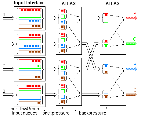
Figure 3: Switching fabric with internal backpressure
If backpressure is not used inside the switching fabric, the designer has to ensure that not too many cells get dropped due to buffer overflows in the fabric; there are two ways to achieve that. First, a large buffer memory can be provided in each switching element in the fabric. To be competitive with the backpressure design, the fabric must be able to operate under heavy load. Then, however, due to traffic burstiness and load fluctuation, the buffers in the switching elements must be very large, thus requiring off-chip memory. Such off-chip buffer per switching element may eliminate the need for the input interfaces, but the buffers introduced at the switching elements are logN times more than the buffers eliminated. At the same time, the off-chip I/O throughput of each switching element is doubled, due to the added off-chip buffer memory. Off-chip communication, in ATLAS I, costs 30% of the chip area and 45% of the chip power (transceivers + elastic interfaces). Doubling that part of the chip in order to eliminate backpressure, which costs less than 10% of the chip area and 4% of the chip power, is a bad idea.
The second method to architect a switching fabric without backpressure and without excessive cell drop rate is to provide internal speed-up: the links in the switching fabric can have s times higher capacity relative to the external links, where s is the speed-up factor. Such a faster fabric, when subject to the same ``heavy'' load as the original fabric, is still lightly loaded relative to its own increased capacity. In this way, the switching elements can have relatively small on-chip buffers, and still achieve a low cell drop rate. The bulk of the queues now accumulate on the output side of the fabric, given that the external links cannot absorb traffic as fast as the fabric can deliver it. What speed-up factor s is required in order to achieve low enough cell drop rates with on-chip buffers? Under a uniform load with non-bursty traffic, a speed-up factor modestly larger than unit would probably suffice. Real traffic, however, is bursty and is not uniformly destined. Even speed-up factors of 1.5 or 2.0 would not be able to ensure low drop rate under large traffic bursts or non-uniformity.
Concerning the cost, a speed-up factor of s is equivalent to multiplying the aggregate link throughput of each switching element by s. In an ATLAS-style chip, this would multiply by s the transceiver and elastic interface cost, and would also multiply by almost s the buffer memory cost (a lot of the buffer cost is due to switching throughput rather than memory capacity). Thus, a speed-up factor of s would roughly cost an extra (s-1.05)*40% in chip area and (s-1.05)*75% in chip power (the .05 in the 1.05 is there to account for the link throughput gained by not having to transmit credits). Obviously, for any realistic speed-up factor s, the added cost of internal speed-up is overwhelmingly larger than the backpressure cost of 10% in chip area and 4% in chip power.
[Cour95] C. Courcoubetis, G. Kesidis, A. Ridder, J. Walrand, R. Weber: ``Admission Control and Routing in ATM Networks using Inferences from Measured Buffer Occupancy'', IEEE Trans. on Communications, vol. 43, no. 4, April 1995, pp. 1778-1784; http://cheetah.vlsi.uwaterloo.ca/ ~kesidis/TComm95.ps
[Efth95] A. Efthymiou: ``Design, Implementation, and Testing of a 25 Gb/s Pipelined Memory Switch Buffer in Full-Custom CMOS'', Technical Report FORTH-ICS/TR-143, ICS, FORTH, Heraklio, Crete, Greece, November 1995; http://archvlsi.ics.forth.gr/switches85-95/ pipeMem_impl25Gbps.ps.gz
[KaSS97] M. Katevenis, D. Serpanos, E. Spyridakis: ``Switching Fabrics with Internal Backpressure using the ATLAS I Single-Chip ATM Switch'', Proceedings of the GLOBECOM'97 Conference, Phoenix, AZ USA, Nov. 1997, pp. 242-246; http://archvlsi.ics.forth.gr/atlasI/ atlasI_globecom97.ps.gz
[KaSS98] M. Katevenis, D. Serpanos, E. Spyridakis: ``Credit-Flow-Controlled ATM for MP Interconnection: the ATLAS I Single-Chip ATM Switch'', Proceedings of HPCA-4 (4th Int. Symposium on High-Performance Computer Architecture) Las Vegas, NV USA, Feb. 1998, pp. 47-56; http://archvlsi.ics.forth.gr/atlasI/ atlasI_hpca98.ps.gz
[KaSV96] M. Katevenis, D. Serpanos, P. Vatsolaki: ``ATLAS I: A General-Purpose, Single-Chip ATM Switch with Credit-Based Flow Control'', Proceedings of the Hot Interconnects IV Symposium, Stanford Univ., CA, USA, Aug. 1996, pp. 63-73; http://archvlsi.ics.forth.gr/atlasI/ atlasI_hoti96.ps.gz
[KaVE95] M. Katevenis, P. Vatsolaki, A. Efthymiou: ``Pipelined Memory Shared Buffer for VLSI Switches'', Proc. of the ACM SIGCOMM '95 Conference, Cambridge, MA USA, Aug. 1995, pp. 39-48; http://archvlsi.ics.forth.gr/switches85-95/ pipeMem_sigcomm95.ps.gz
[Korn97] G. Kornaros, C. Kozyrakis, P. Vatsolaki, M. Katevenis: ``Pipelined Multi-Queue Management in a VLSI ATM Switch Chip with Credit-Based Flow Control'', Proc. 17th Conference on Advanced Research in VLSI (ARVLSI'97), Univ. of Michigan at Ann Arbor, MI USA, Sept. 1997, pp. 127-144; http://archvlsi.ics.forth.gr/atlasI/ atlasI_arvlsi97.ps.gz
[Man97] ``ATLAS I Architecture Manual'', ICS-FORTH, Crete, Greece, 1997; Internal ASICCOM working document; to be published on-line at a later time, under the directory: http://archvlsi.ics.forth.gr/atlasI/
[MCLN93] R. Marbot, A. Cofler, J-C. Lebihan, R. Nezamzadeh: ``Integration of Multiple Bidirectional Point-to-Point Serial Links in the Gigabits per Second Range'', Hot Interconnects I Symposium, Stanford Univ., CA, USA, Aug. 1993.
[QFC95] Quantum Flow Control Alliance: ``Quantum Flow Control: A cell-relay protocol supporting an Available Bit Rate Service'', version 2.0, July 1995; http://www.qfc.org